
 Tel:+86-13713635953
 Email:support@quicko.com.cn


SMD Soldering Guide: Tools, Tips, and Techniques
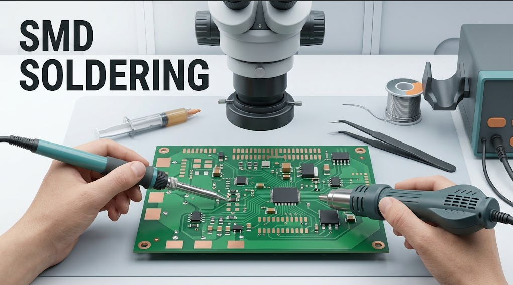
SMD Soldering Guide: Tools, Tips, and Techniques
SMD soldering is the controlled process of attaching surface-mount components directly to PCB pads with solder, flux, heat, and accurate positioning. For prototypes and repairs, the most reliable approach is to secure the board, use magnification, select a tip or nozzle that transfers heat efficiently, tack the component in alignment, complete the joints with fresh flux, and inspect the result before power is applied.This SMD soldering guide is for hobbyists learning small-component work, technicians handling PCB rework, production teams documenting a manual process, and buyers assembling a precision bench. It covers hand soldering, drag soldering, hot-air removal and replacement, inspection, and defect correction. It does not replace the component datasheet, PCB assembly drawing, solder-alloy guidance, equipment manual, or your organization's ESD and safety procedure.
Commercial disclosure: QUICKO publishes this guide and sells soldering stations, handles, cartridges, and tips. QUICKO links are commercial links. The technical workflow is kept separate from model-specific claims, and no product is presented as suitable for every board or package.
Quick Answer: What Is the Best Way to Solder SMD Components?
For a two-terminal chip component, apply flux, lightly tin one pad, reflow that pad while positioning the component, then solder the opposite termination. Revisit the first joint only if its wetting or alignment needs correction. For fine-pitch gull-wing packages, tack opposite corners and use drag soldering with abundant flux and a controlled solder film. Use hot air when all terminations must become molten together or when removal with an iron would load the pads mechanically.The correct method is package dependent. A resistor, a QFP with exposed leads, and a bottom-terminated QFN do not present the same access or inspection problem. If a joint is hidden beneath the package, a validated paste-and-reflow or controlled hot-air process may be more appropriate than an iron-only technique.
Table of Contents
- What SMD soldering includes
- Tools and bench setup
- Choosing a tip, cartridge, and hot-air nozzle
- Hand-soldering chip components
- Drag soldering fine-pitch ICs
- Hot-air PCB rework
- Inspection and quality checks
- Common defects and fixes
- Process control for repeatable work
- Buyer checklist
- Frequently asked questions
What SMD Soldering Includes
Surface-mount devices sit on conductive pads rather than passing leads through drilled holes. The package may expose metal end caps, gull-wing leads, J-leads, tabs, or only pads beneath the body. That geometry decides what the operator can heat, see, clean, and inspect.Adafruit's surface-mount component soldering walkthrough demonstrates the core hand-soldering sequence: immobilize the part, heat the pad and termination, feed solder to the joint rather than the tip alone, and allow the joint to cool without movement. That pattern works well for accessible terminations, but it is only one part of SMD work.
| Method | Best fit | Main control | Typical failure to prevent |
|---|---|---|---|
| Point or chisel hand soldering | Chip resistors, capacitors, diodes, accessible leads | Tip contact, solder quantity, alignment | Tombstoning, disturbed joints, excess solder |
| Drag soldering | Fine-pitch gull-wing ICs | Flux, solder film, tip path, lead alignment | Bridges and unsoldered leads |
| Hot-air rework | Multi-lead removal, replacement, bottom-terminated packages | Airflow, heat distribution, shielding, lift timing | Shifted neighbors, overheated laminate, lifted pads |
| Paste and controlled reflow | Repeated assembly or hidden terminations | Paste deposit, placement, thermal profile | Opens, shorts, voiding, package damage |
Soldering creates a joint. Rework changes an existing assembly. Rework therefore adds removal risk, old solder and flux residues, unknown prior heat exposure, damaged pads, conformal coating, nearby plastic, and the possibility that the original defect has another cause. Treat the two jobs differently.
SMD Soldering Tools and Bench Setup
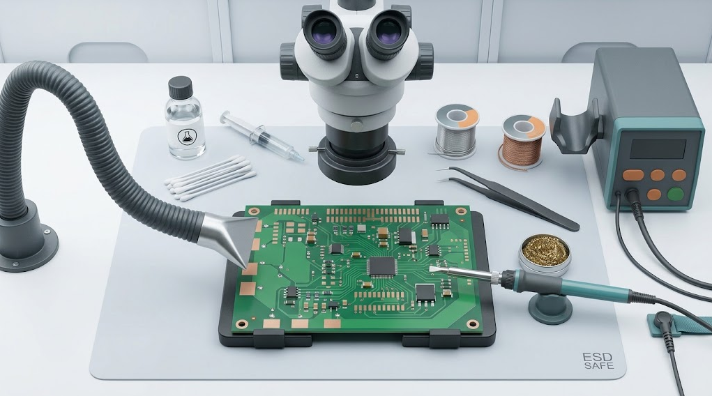
A precision station matters, but a station alone does not make a usable bench. The Adafruit soldering-tool guide groups the iron with a stand, appropriate solder, cleaning tools, workholding, solder wick, and extraction. For SMD work, add magnification, fine component handling, ESD controls, and inspection lighting.Core equipment
- Temperature-controlled soldering station: Use a stable system with documented cartridge or tip support, a safe stand, sleep behavior, and grounding appropriate to the work.
- Useful tip shapes: Start with a small chisel for chip parts and individual leads. Add a bevel or hoof geometry for drag soldering when the package and process support it. Avoid choosing a needle point simply because the component is small; inadequate contact can lengthen dwell time.
- Hot-air station: Look for predictable control, interchangeable nozzles, a stand or cradle, and airflow that remains stable at the chosen setting.
- Magnification and light: Use enough magnification to see pad edges, lead alignment, solder bridges, debris, and disturbed joints without forcing an awkward posture.
- Fine tweezers and board support: Straight and curved ESD-safe tweezers cover most placement tasks. A rigid low-profile holder prevents the board from moving while preserving access.
- Flux and solder: Use electronics-grade materials compatible with the alloy, finish, cleaning process, and reliability requirement. Plumbing flux is not suitable for electronics.
- Rework supplies: Keep fresh solder wick, a flux applicator, lint-free swabs, an approved cleaning solvent, heat-resistant tape or shields, and spare practice boards at the bench.
Safety and contamination control
Disconnect power and remove energy sources before rework. Wear eye protection, keep hot tools in their stands, and keep flammable materials away. Use local extraction close enough to capture flux fume without blowing across the joint or cooling the work unpredictably.The UK Health and Safety Executive's guidance on rosin-based solder flux fumes warns that rosin fume can cause serious health problems and discusses local exhaust ventilation. If leaded solder is used, follow the applicable workplace rules, keep food and drink away, wash hands, and prevent residues from leaving the work area. The US National Institute for Occupational Safety and Health explains in its workplace lead exposure overview that lead exposure can cause health problems and can be carried home on clothes and other items.
Do not assume a “no-clean” flux means every residue is harmless in every electrical, optical, high-impedance, or coating process. Follow the flux manufacturer's cleaning guidance and the assembly's reliability requirement. For cleaning where the process permits it, iFixit lists high-concentration isopropyl alcohol above 90% with a soft brush in its soldering and desoldering guide; confirm solvent compatibility with plastics, labels, coatings, and adhesives first.
Choosing a Soldering Tip, Cartridge, and Hot-Air Nozzle
The best iron tip is usually the largest face that fits the exposed metal without touching adjacent parts. A chisel can contact the pad and termination at the same time, creating a broader thermal bridge than a sharp cone. A bevel or hoof can hold a small solder film for drag soldering. Long, thin shapes improve reach but may transfer heat less efficiently than shorter shapes in the same family.Choose by four constraints:
- Contact: Can the working face touch both conductors without forcing the tool into the board?
- Clearance: Can the operator see and reach the joint without contacting nearby plastic, coating, or components?
- Thermal load: Does the joint connect to a large copper area, shield, connector, or internal plane that pulls energy away?
- Process control: Can the station, handle, cartridge, and tip recover predictably within the documented limits?
How to Hand-Solder SMD Chip Components
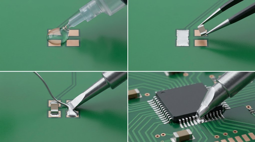
Practice on a scrap board before working on valuable hardware. Verify the component value, polarity, orientation, and pad condition under magnification. Then use this seven-step process for a two-terminal resistor, capacitor, diode, or similar part with accessible end terminations.- Prepare the pads. Remove contamination and old residue using an approved method. If this is a repair, inspect for lifted copper, missing solder mask, or pad damage before continuing.
- Apply a small amount of flux. Coat the joint area without flooding adjacent components or connectors.
- Tin one pad lightly. Create a small, controlled solder deposit. A large dome will hold the component above the board and make alignment difficult.
- Place and tack the component. Hold the body with tweezers, reflow the tinned pad, and lower the termination into the molten solder. Remove the iron, keep the part still, and allow the joint to solidify.
- Check alignment. Confirm that both terminations overlap their pads, the component is flat enough for the design, and polarity is correct. Reposition now, before the second joint locks the part in place.
- Solder the second termination. Touch the pad and metal termination together with the tip, then feed only enough solder to create a wetted fillet. Remove solder, then remove heat.
- Revisit and inspect. Refresh flux and correct the first joint only if required. Clean as specified and inspect both ends under magnification.
How to Drag-Solder Fine-Pitch ICs
Drag soldering works on exposed gull-wing leads when the package is aligned and the operator can see the lead-to-pad interface. It is not a substitute for a validated process on bottom-terminated packages.- Apply flux across the pads and leads.
- Align the package, then tack two opposite corner leads.
- Recheck every side under magnification. Correct rotation or offset before adding more joints.
- Load a small solder film onto a suitable bevel, hoof, or small chisel.
- Draw the tip along the lead ends with light contact and a steady path. Let flux and surface tension help distribute solder.
- Inspect for bridges, dry leads, bent pins, and solder balls. Add flux before attempting a correction.
Hot-Air PCB Rework: Remove and Replace Without Forcing
Hot-air rework should heat all target joints together and let the component release without mechanical force. Before starting, identify heat-sensitive plastics, microphones, cameras, displays, batteries, adhesives, shields, connectors, and small neighboring parts. Shield or remove vulnerable items as the approved process requires.Removal workflow
- Document component orientation and the original defect with a photograph or board map.
- Secure and support the assembly. Preheat only when the board, package, and approved process call for it.
- Apply flux to the target joints and select a nozzle that concentrates heat without covering unnecessary area.
- Establish airflow before approaching the board. Keep a controlled standoff and motion pattern rather than dwelling on one corner.
- Test release with the lightest possible tweezer touch. Lift vertically only after every joint is molten.
- Stop if the package resists. More pulling is not a substitute for complete reflow and can remove pads.
- Let the board cool according to the process, then clean and inspect the site before pad preparation.
Replacement workflow
Prepare the pads without scraping copper or removing more solder than necessary. Apply the approved flux or paste, align the replacement using package and board landmarks, and heat evenly. Watch for the component to settle as the joints reflow, but do not assume visible movement proves every hidden joint is acceptable. Allow the assembly to cool undisturbed, then inspect and test using criteria appropriate to the package.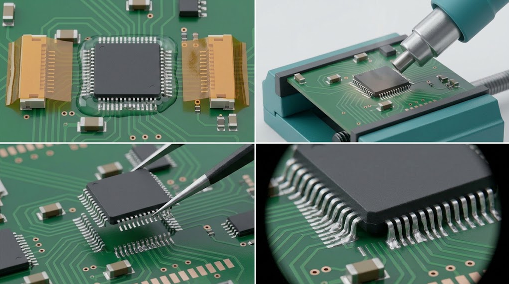
SMD Joint Inspection and Quality Checks
Inspect before electrical power is restored. Visual inspection cannot prove the quality of every hidden joint, but it can catch alignment errors, bridges, debris, disturbed solder, incomplete wetting, lifted pads, and damaged components.| Check | Acceptable direction | Investigate or rework |
|---|---|---|
| Alignment | Terminations overlap the intended pads; polarity and pin 1 are correct | Offset, rotation, reversed polarity, lead off pad |
| Wetting | Solder follows the pad and termination with a coherent fillet | Bead sitting on one surface, exposed unwetted interface |
| Solder quantity | Enough to form the joint while preserving the outline needed for inspection | Bridge, ball, bulky mound, or visibly starved connection |
| Component condition | Body, leads, pads, mask, and nearby parts remain intact | Cracked body, bent lead, scorched laminate, lifted pad |
| Cleanliness | Residues meet the flux and assembly requirements | Conductive debris, loose solder balls, incompatible residue |
| Electrical result | No unintended short; expected continuity and function after safe checks | Short circuit, intermittent connection, unexpected leakage |
For production or high-reliability work, use the drawing, customer specification, applicable workmanship standard, and trained inspection method. Bottom-terminated packages may require X-ray, functional tests, boundary scan, or other process controls because the joints cannot be assessed fully from the side.
Common SMD Soldering Defects and Fixes
Solder will not wet the pad or lead
Stop adding solder. Clean the surfaces, verify the pad and termination are solderable, add compatible fresh flux, clean and tin the tip, and improve contact geometry. If a larger tip face fits safely, it may transfer heat more efficiently than raising the setpoint. Replace a damaged or oxidized component rather than repeatedly heating it.The component moves when the iron leaves
The part moved before the joint solidified or was never secured. Reflux, reflow one joint, hold the part in alignment without excess pressure, remove heat, and keep the tweezers still until the solder sets. Improve board support if hand motion is being transferred to the joint.Fine-pitch leads are bridged
Check alignment first; a displaced package cannot be repaired by removing solder alone. Add flux, use a clean tip to pull excess solder toward the end of the row, then use fresh wick if needed. Inspect the entire row again because correcting one bridge can disturb a neighboring lead.A pad starts to lift
Stop heating and stop pulling. Let the board cool, document the damage, and assess whether the pad, trace, or via can be repaired under an approved procedure. A lifted pad is a structural defect, not a cosmetic issue. Repeated reheating without a repair plan usually makes it worse.Nearby parts shift during hot-air work
Reduce unnecessary heated area, review nozzle size and airflow, improve shielding, and stabilize loose parts only with an approved method. Consider board preheat where permitted so the top-side tool does not have to create the entire temperature rise locally.Make PCB Rework Repeatable
A remembered knob position is not a process record. For repeated boards, create a short traveler or worksheet that records:- Board revision, component designator, package, and defect type
- Solder alloy, flux, cleaning material, and lot where traceability is required
- Iron cartridge family, tip shape, and working-face width in millimeters
- Setpoint in degrees Celsius, contact time in seconds, and number of heating cycles
- Hot-air nozzle diameter in millimeters, airflow setting, standoff, motion pattern, and preheat condition
- Shielding method, inspection method, acceptance criteria, and result
- Operator, equipment ID, calibration status, date, and reviewer where required
SMD Soldering Station Buyer Checklist
Buy for the joints and packages that appear on the bench, not for the largest wattage printed in a listing. Evaluate the complete system:- Cartridge and tip shapes that cover chip parts, individual leads, drag soldering, and moderate thermal loads
- Working distance and grip-to-tip geometry under your microscope
- Controller behavior, recovery, calibration support, sleep, and hibernation
- Tip-to-ground performance and ESD controls appropriate to the assemblies
- Hot-air nozzle range, airflow stability, handpiece stand, and service parts
- Local voltage, plug, supply, isolation, grounding, documentation, and warranty
- Replacement cartridges, handles, heaters, nozzles, stands, and consumables
Frequently Asked Questions
What soldering tip is best for SMD work?
A small chisel is the best general starting shape because it can contact a pad and component termination together. Use the largest face that fits without touching neighbors. Add a bevel or hoof for drag soldering if the process supports it. A needle point improves access but may transfer heat poorly and increase dwell time.Do I need hot air for SMD soldering?
No. An iron and tweezers can handle many chip components and exposed-lead packages. Hot air becomes valuable when several joints must reflow together, a component must be removed without loading individual pads, or terminations sit beneath the package. Hidden joints may also require paste, controlled reflow, and inspection beyond a microscope.What temperature should I use for SMD soldering?
There is no universal setpoint. Start with the station, solder-alloy, flux, component, and assembly guidance, then validate on representative work. Tip shape, calibration, copper mass, contact area, and preheat affect the required setting. If a joint heats slowly, improve contact and geometry before automatically increasing temperature.How do I prevent tombstoning when hand-soldering chip parts?
Control one end at a time. Lightly tin one pad, reflow it while positioning the component flat, let that joint solidify, then solder the second end. Avoid large solder deposits and unnecessary reheating of both sides. In paste reflow, pad design, paste balance, placement, wetting, and the thermal profile also affect tombstoning.Can I inspect every SMD joint visually?
No. Exposed leads and chip terminations provide useful visual evidence, but joints under QFN, BGA, LGA, and similar packages are hidden. Depending on risk, the process may need X-ray, electrical tests, boundary scan, functional tests, thermal checks, or validated process controls. Use the product and quality requirements to choose the inspection method.Conclusion
Reliable SMD soldering comes from controlling the whole path: a stable board, visible joints, compatible materials, useful tip or nozzle geometry, enough flux, minimal mechanical force, documented settings, and inspection before power-up. Hand soldering is efficient for accessible chip parts and leads, drag soldering speeds aligned fine-pitch rows, and hot air is the safer choice when all terminations must release together.Build the process around representative boards rather than a universal recipe. Start with the largest safe contact face, protect nearby materials, record what worked, and stop when a part resists instead of pulling harder. To assemble a QUICKO precision soldering and PCB rework setup, match the station, handpiece, cartridge, tip shapes, hot-air capability, ESD controls, and inspection tools to your actual package mix and thermal loads.


Linkedin:


